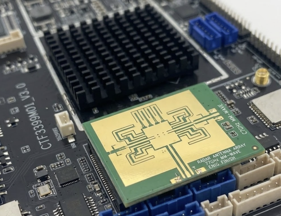
SHENZHEN, GUANGDONG, CHINA, October 12, 2026 /EINPresswire.com/ — The automotive industry continues to advance its Advanced Driver Assistance Systems to achieve higher autonomous driving capabilities. Hardware engineers are actively shifting radar operating frequencies from 24GHz to 77GHz and 79GHz bands to improve spatial resolution. This frequency migration allows sensors to detect smaller objects with exceptional accuracy at longer distances. However, operating at these ultra-high frequencies introduces severe physical and electromagnetic constraints for circuit designers. Specifically, high-frequency signals trigger the skin effect phenomenon, which forces electrical current to travel only along the outermost boundary of a conductor. Because of this phenomenon, signal loss becomes highly sensitive to circuit surface roughness and plating discrepancies. Therefore, modern Tier-1 automotive integrators must choose a High Quality Gold-Plated One-Stop PCBA Manufacturer to safeguard signal propagation. Advanced chemical surface finishes provide the necessary microscopic flatness to protect radio frequency waves from degradation. Ultimately, selecting a highly specialized assembly partner establishes the ultimate foundation for manufacturing zero-defect automotive safety components.
Benefit 1: Optimizing High-Frequency Conduction and Minimizing Skin-Effect Attenuation
Conventional circuit board finishes like Hot Air Solder Leveling frequently create uneven surfaces across microstrip patch antennas. These microscopic irregularities scatter ultra-high-frequency waves, which leads to massive signal attenuation in the radar transceiver circuit. To resolve this performance bottleneck, advanced automotive radar systems deploy Electroless Nickel Immersion Gold surface finishes. This specific plating process creates an exceptionally flat, atom-thick gold layer over the copper circuitry. Consequently, the uniform golden surface provides a perfectly smooth pathway for high-frequency millimeter-wave signals to travel without distortion. Accurate process control during the chemical immersion phase determines the ultimate transmission efficiency of the sensor hardware. For instance, Aozite OST PCBA precisely regulates its automated chemical deposition lines to maintain gold thickness within an optimal range of 0.05 to 0.1 microns. This thin layer seals a protective three-to-five-micron nickel undercoat without introducing unwanted structural variations. As a result, the radar module achieves excellent signal consistency across all antenna channels. By eliminating surface roughness, this advanced plating approach minimizes insertion losses during high-speed data processing cycles.
Benefit 2: Minimizing Parasitic Capacitance and Securing Impedance Matching in Dense Arrays
Millimeter-wave radar transceivers require perfect impedance matching along every transmission track to maintain high object detection sensitivity. Any physical variance in trace width or plating thickness shifts the characteristic impedance away from the standard 50-Ohm target value. Such impedance mismatches generate destructive signal reflections, which drastically lower the operational range of the radar sensor. Furthermore, uneven metal coatings introduce unwanted parasitic capacitance along closely spaced circuit edges. This parasitic noise disrupts the precise phase timing required for modern digital beamforming arrays. If phase errors occur, the radar unit may generate ghost targets or fail to track moving obstacles accurately. To mitigate these electrical risks, specialized factories implement rigid geometric tolerance controls during circuit manufacturing. This manufacturing precision matches the high standards seen in a one-stop PCBA turnkey solution for industrial control and automation equipment. Advanced optical measurement systems continuously verify track geometries down to the micron level during production. By enforcing uniform chemical gold distribution across dense multi-channel antenna arrays, the fabrication process suppresses parasitic capacitance effectively. This strict electrical discipline guarantees that the finished radar modules maintain uncompromised phase accuracy during complex road environments.
Benefit 3: Mitigating Black Pad Vulnerabilities to Maximize Solder Joint Mechanical Strength
High-quality surface finishing must balance superior electrical performance with robust structural durability. During substandard gold plating processes, excessive phosphorus enrichment often occurs at the boundary between the gold and nickel layers. This defect causes the notorious black pad phenomenon, which severely weakens the underlying metallic bond. Consequently, the vulnerable circuit connections can easily develop micro-cracks under continuous vehicle road vibrations or sudden mechanical impacts. To prevent this severe structural hazard, manufacturing engineers must optimize the formation of the intermetallic compound during the reflow process. A proper nickel-tin crystal structure, specifically Ni3Sn4, creates highly resilient and shock-resistant solder joints beneath heavy ball grid array radar chips. For this reason, Aozite OST PCBA (Shenzhen Aozite Technology Co., Limited) utilizes strict cross-sectional analysis alongside automated X-ray testing. These advanced non-destructive inspections ensure that the intermetallic layer grows uniformly without hidden structural voids. By checking the microscopic integrity of every solder joint, the factory completely eliminates brittle fracture risks. This meticulous engineering focus maximizes the mechanical shear strength of the assembly, ensuring the sensor remains operational throughout the vehicle lifecycle.
Benefit 4: Establishing Hermetic Oxidation Resistance for Lifelong Automotive Harsh-Environment Survival
Automotive radar sensors usually sit directly behind vehicle bumpers or front grilles, exposing them to incredibly harsh working environments. The assembly must withstand continuous thermal cycling, extreme atmospheric humidity, road salt spray, and chemical contaminants. Therefore, exposed circuit pads require an airtight barrier to prevent copper oxidation and environmental degradation over time. Immersion gold operates as an ideal, non-porous chemical shield because gold remains completely inert under normal atmospheric conditions. This protective layer perfectly seals the underlying nickel and copper materials from moisture penetration. Furthermore, high-quality ENIG finishes maintain excellent solder wettability even after experiencing multiple thermal assembly cycles in multi-zone reflow ovens. This robust thermal resistance allows factories to execute complex double-sided surface mount processes without degrading unpopulated pads. By preventing corrosion at the exposed pad boundaries, the chemical finish ensures the radar unit retains its structural integrity for a fifteen-year lifespan. This long-term reliability remains crucial for autonomous safety systems that must operate flawlessly without constant maintenance interventions.
Benefit 5: Closed-Loop Turnkey Execution and Strict Supply Chain Traceability for Zero-Defect Manufacturing
Sourcing printed circuit boards, electronic components, and surface-mount processing from separate vendors introduces massive quality control risks. Fragmented supply chains often suffer from communication gaps, material inconsistencies, and untraceable component defects. Conversely, a closed-loop turnkey manufacturing framework unifies engineering review, material sourcing, plating control, and automated assembly under a single system. This integrated methodology eliminates external variables and ensures consistent radio frequency performance across mass production batches. Global automotive integrators benefit significantly when a single professional partner manages the complete manufacturing pipeline from raw materials to functional verification. To ensure zero-defect output, Shenzhen Aozite Technology Co., Limited operates eight high-speed automated SMT lines with a total daily capacity exceeding 1.2 million solder points. The manufacturing center utilizes integrated manufacturing execution systems to laser-mark unique tracking codes onto every board. This database tracks each active and passive component back to its original factory production batch, completely blocking counterfeit materials. By combining rigorous plating technology with comprehensive turnkey execution, professional Chinese facilities help global automotive innovators scale up production safely and capture emerging market opportunities.
For more information regarding advanced automotive manufacturing capabilities and technical services, please visit the official corporate portal: https://www.aozite-pcba.com/.
Aozite OST PCBA
Aozite OST PCBA
Legal Disclaimer:
EIN Presswire provides this news content “as is” without warranty of any kind. We do not accept any responsibility or liability
for the accuracy, content, images, videos, licenses, completeness, legality, or reliability of the information contained in this
article. If you have any complaints or copyright issues related to this article, kindly contact the author above.

Media gallery